
Logic Gate Basics Using Transistors
2025-03-15

How RTL NAND Gates Work with NPN Transistors
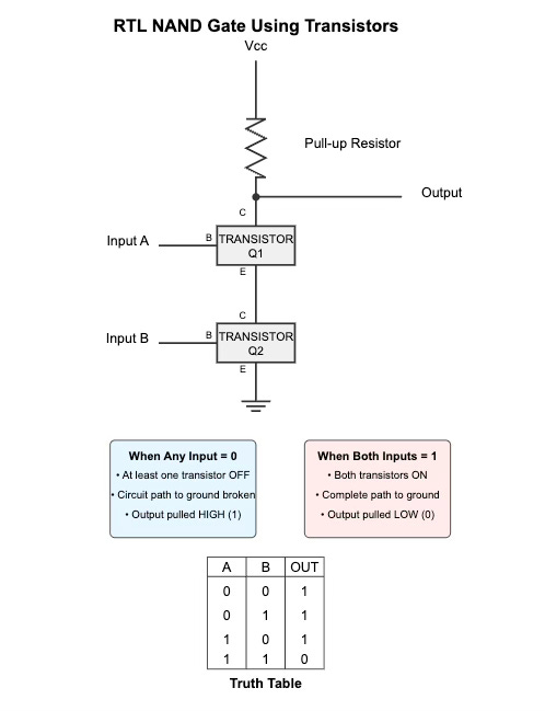
Resistor-Transistor Logic (RTL) was one of the earliest forms of digital logic used in early computers. Let me explain how an RTL NAND gate works using NPN transistors.
Circuit Structure
As shown in the diagram, an RTL NAND gate consists of:
A pull-up resistor connected to the power supply (Vcc)
Two NPN transistors (Q1 and Q2) connected in series
The collector of Q1 connected to the output node
The emitter of Q1 connected to the collector of Q2
The emitter of Q2 connected to ground
How It Works
The operation of this RTL NAND gate depends on the states of both transistors:
Case 1: Any Input = 0 (LOW)
When either Input A OR Input B is LOW (0V)
The corresponding transistor is OFF (not conducting)
The path from output to ground is broken
The pull-up resistor pulls the output voltage HIGH to Vcc
Result: Output = 1 (HIGH)
Case 2: Both Inputs = 1 (HIGH)
When both Input A AND Input B are HIGH (+V)
Both transistors turn ON (conducting)
A complete path forms from output to ground
Current flows through both transistors to ground
The output voltage is pulled LOW
Result: Output = 0 (LOW)
Key Features of RTL NAND Gates
Series Connection: The transistors are in series, creating an AND function for the path to ground.
Inversion: The output is inverted due to the pull-up resistor, turning the AND function into NAND.
Fan-out Limitation: The output's ability to drive multiple gates is limited by the pull-up resistor value.
Speed Limitation: The RC time constant created by the pull-up resistor and parasitic capacitances limits switching speed.
Historical Significance
RTL was used in early integrated circuits like the Apollo Guidance Computer and early IBM computers. While it has been superseded by more advanced logic families (TTL, CMOS), understanding RTL helps grasp the fundamental principles of digital logic implementation.
This series connection of transistors illustrates a fundamental principle in digital logic design: placing switches in series implements an AND function, while the pull-up resistor creates the inversion needed for NAND operation.
How RTL NOR Gates Work with Transistors
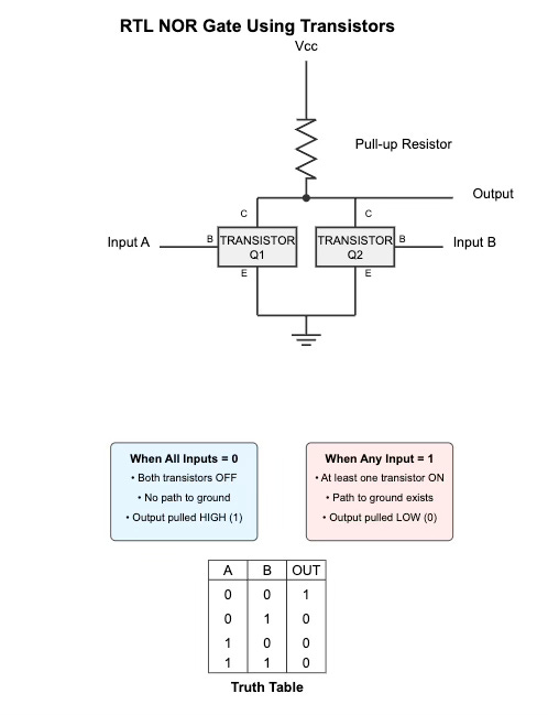
A NOR gate is another fundamental digital logic gate that combines the OR and NOT operations. The output is HIGH only when both inputs are LOW. I'll explain how Resistor-Transistor Logic (RTL) implements a NOR gate using transistors.
Circuit Structure
As shown in the diagram, an RTL NOR gate consists of:
A pull-up resistor connected to the power supply (Vcc)
Two transistors connected in parallel (key difference from NAND)
Each transistor's collector connected to the output node
Each transistor's emitter connected to a common ground rail
Each transistor's base connected to a separate input
How It Works
The operation of this RTL NOR gate depends on the states of both transistors:
Case 1: All Inputs = 0 (LOW)
When both Input A AND Input B are LOW (0V)
Both transistors are OFF (not conducting)
No path exists from output to ground
The pull-up resistor pulls the output voltage HIGH to Vcc
Result: Output = 1 (HIGH)
Case 2: Any Input = 1 (HIGH)
When either Input A OR Input B is HIGH (+V)
At least one transistor turns ON (conducting)
A path forms from output to ground through the conducting transistor(s)
Current flows through the transistor(s) to ground
The output voltage is pulled LOW
Result: Output = 0 (LOW)
Key Differences from NAND
Parallel vs. Series Connection:
NOR: Transistors are connected in parallel (either can pull the output LOW)
NAND: Transistors are connected in series (both must be ON to pull the output LOW)
Logical Operation:
NOR implements (NOT OR): Output is HIGH only when all inputs are LOW
NAND implements (NOT AND): Output is LOW only when all inputs are HIGH
Circuit Characteristics
Fan-out: The NOR gate's ability to drive multiple gates depends on the pull-up resistor value.
Speed: The switching speed is limited by the RC time constant created by the pull-up resistor and parasitic capacitances.
Power Consumption: When any input is HIGH, there's continuous current flow from Vcc through the pull-up resistor and active transistor(s) to ground.
Expandability: Additional inputs can be added by connecting more transistors in parallel to the same output node.
This parallel connection of transistors illustrates another fundamental principle in digital logic design: placing switches in parallel implements an OR function, while the pull-up resistor creates the inversion needed for NOR operation.
NOT Gate
See the previous article.
See Also
Email: ptcomputingsimplicity@gmail.com
References: https://guitarvydas.github.io/2024/01/06/References.html
Blog: guitarvydas.github.io
Videos: https://www.youtube.com/@programmingsimplicity2980
Discord: https://discord.gg/65YZUh6Jpq
Leanpub: [WIP] https://leanpub.com/u/paul-tarvydas
Gumroad: tarvydas.gumroad.com
Twitter: @paul_tarvydas
Substack: paultarvydas.substack.com