


How A Transistor Makes A Logic Inverter
2025-03-15

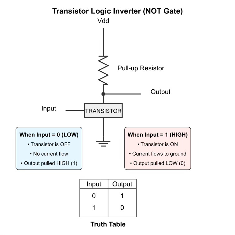
A transistor can function as a logic inverter (also called a NOT gate) by using its switching properties to convert a logical HIGH input to a LOW output, and vice versa. Let me explain how this works using an NPN transistor as an example.
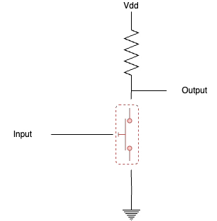
Analogy: Push Button Instead of Transistor
How a Transistor Inverter Works
When using a transistor as a logic inverter:
Basic Setup: A transistor is connected with its emitter to ground, its collector to a resistor (which connects to power supply Vdd), and its base receives the input signal.
Input LOW (0): When the input voltage is LOW (logical 0):
The transistor is OFF (not conducting)
Current cannot flow through the transistor
The output voltage is pulled UP to Vdd through the resistor
Result: Output is HIGH (logical 1)
Input HIGH (1): When the input voltage is HIGH (logical 1):
The transistor turns ON (conducting)
Current flows through the transistor to ground
The output voltage is pulled DOWN close to ground
Result: Output is LOW (logical 0)
This creates the inverting behavior where: Input 0 → Output 1, and Input 1 → Output 0.
Practical Considerations
Resistor Value: The pull-up resistor's value is critical for proper operation. It needs to be:
Large enough to limit current when the transistor is ON
Small enough to ensure a fast transition to HIGH when the transistor turns OFF
Propagation Delay: There's a small delay between input and output changes due to the charging/discharging of parasitic capacitances.
Power Consumption: When the input is HIGH and transistor is ON, there's continuous current flow through the resistor to ground, which consumes power.
Modern Implementation: In modern integrated circuits, this basic transistor inverter has evolved into CMOS (Complementary Metal-Oxide-Semiconductor) inverters, which use both NMOS and PMOS transistors to reduce power consumption and improve performance.
This simple circuit forms the foundation of digital logic and is a building block for more complex gates and circuits in digital electronics.
[Note: the language used in this note is approximate and is only intended to give a flavour for how these things operate. Some details have been conflated together and glossed over. For example TTL circuits usually use the name Vcc instead of Vdd. Vdd is more common in MOS circuitry. Those kinds of details are unimportant in this overview.]
[More details can be found in the appendices of the PDF version of this article.]
See Also
Email: ptcomputingsimplicity@gmail.com
References: https://guitarvydas.github.io/2024/01/06/References.html
Blog: guitarvydas.github.io
Videos: https://www.youtube.com/@programmingsimplicity2980
Discord: https://discord.gg/65YZUh6Jpq
Leanpub: [WIP] https://leanpub.com/u/paul-tarvydas
Gumroad: tarvydas.gumroad.com
Twitter: @paul_tarvydas
Substack: paultarvydas.substack.com